Practical Op Amp Integrator Circuit Circuit Diagram An op-amp integrator is a critical part of ADCs, analog computers, and even wave-shaping circuits. While not as common as the voltage follower , comparator , and inverting/non-inverting amplification configurations, the integrator circuit is a great circuit to have in your back pocket.

Key learnings: Op-Amp Integrator Definition: An op-amp integrator is a circuit that uses an operational amplifier and a capacitor to calculate the integral of an input signal, outputting a voltage that reflects the cumulative effect of the input signal over time.; Function: The primary function of an op-amp integrator is to convert waveforms, such as turning a square wave into a triangular The integrator op amp circuit we will build with an LM741 op amp chip is shown below. Below is the breadboard circuit of the circuit shown above. So, when there is a resistor at the input to the inverting terminal and a resistor and capacitor are in parallel with one side connected to the inverting terminal and the other side to the output, we

How to design practical Op Circuit Diagram
Integrator circuit is exactly opposite of Op-amp differentiator circuit. A simple Op-amp configuration consists of two resistors, which creates a feedback path. In the case of Integrator amplifier, the feedback resistor is changed with a capacitor. In the above image, a basic integrator circuit is shown with three simple components. The
2. Select a CMOS op amp to minimize the errors from the input bias current. 3. The gain bandwidth product (GBP) of the amplifier will set the upper frequency range of the integrator function. The effectiveness of the integration function is usually reduced starting about one decade away from the amplifier bandwidth. 4. For the LM358 op-amp based integrator design, let us consider that the input signal amplitude is 100mV and frequency is 1KHz. Let us use single supply voltage 5V for LM358 op-amp. Also let us consider that the output signal should swing around 2.5V. Let the DC gain of an integrator be 10. The LM358 based integrator circuit diagram is shown below. An operational amplifier (op-amp) integrator circuit is essential in analog signal processing applications such as waveform generation, analog computation, and filtering. In this post, we will walk through the design calculation of a practical op-amp integrator using the LM358 op-amp, with a specified integration time of 25 ms. Additionally, we

Design Calculation for Practical Op-Amp Integrator Circuit Diagram
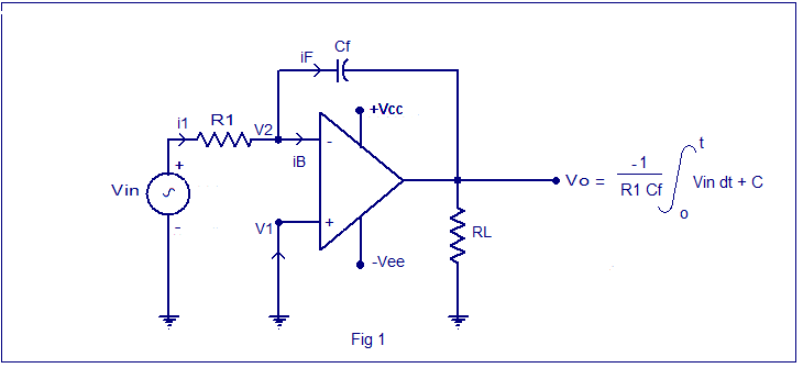
An operational amplifier integrator circuit produces an output voltage which is proportional to the area (amplitude multiplied by time) contained under the waveform. An ideal op-amp integrator uses a capacitor C f , connected between the output and the op-amp inverting input terminal, as shown in the figure below. The practical op-amp integrator differs from basic or ideal integrator circuit in that a resistor RF is used in parallel with the capacitor CF. Also a bias resistor Rb is used. The resistor RF minimizes the problem due to offset voltage and the resistor Rb minimizes the problem due to bias current. Where: ω = 2πƒ and the output voltage Vout is a constant 1/RC times the integral of the input voltage V IN with respect to time. Thus the circuit has the transfer function of an inverting integrator with the gain constant of -1/RC. The minus sign ( - ) indicates a 180 o phase shift because the input signal is connected directly to the inverting input terminal of the operational amplifier.
