Simplified schematic of the highvoltage level shifter Circuit Diagram The level shifter (LS) circuit has become an indispensable circuit component in both analog and digital systems. In the past decades, there has been an exponential increase in the academic publications for the LS circuits to improve their performances and their applications. Therefore, this review paper provides a comprehensive study of the LS circuit, ranging from circuit topologies and It may get damaged, so we need logic level shifter. Let's make a simple logic level shifter using two npn transistors. These types of level shifter are widely use in many of the digital devics. In this instructables we are going to design a simple circuit of level shifter just for understanding how they works. Practically cmos are preferred for

So R1 and R2 form a voltage divider, and R2 should be twice R1 to get the 0 V. Next we have to find the amplification, which is determined by R3 and R4: (the "to_adc" is the output voltage): The above non-inverting circuit is a bit like your summing amplifier. (e.g. > 5k) you will need to buffer the signal before sending to the level
DIY 5v to 3.3v Logic Level Shifter : 3 Steps Circuit Diagram
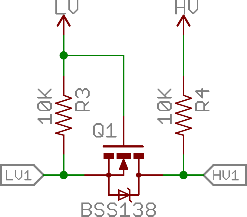
A logic level shifter, or a voltage level translator, is used to translate signals from one logic level to another. Nowadays, most of the system runs on 3.3V or 5V. Logic level is simply a HIGH and LOW level of voltage for a certain board or IC. Design a 5V to 3.3V Translation Circuit. To translate 5V signals to 3.3V signals, the simplest The simplest and most common method of logic level shifting is a voltage divider. In the circuit shown as in the first picture, the output of the divider is the line coming out from the middle. There is a total of 5V dropped across the circuit, but we can can calculate how much voltage is dropped across each resistor. In the logic level shifter circuit shown above, consider that the MOSFET turns on fully when we supply a Gate-Source voltage (V GS) of 3.3 Volts. Low-level to high-level conversion: When the voltage at point A is at 3.3V, the MOSFET stays in the cut-off region as the voltage difference between the Gate and Source is less than the threshold

A level shifter circuit is used to convert signals from one voltage level to another while maintaining the shape of the signal. This is commonly needed when interfacing different parts of a system that operate at different voltage levels, such as between microcontrollers, sensors, or other integrated circuits. A level shifter is an electronic device that changes the voltage level of signals between different logic circuits or microcontrollers. The main purpose of using a level shifter is to ensure compatibility between components that Level Shifter Circuits - Design Basics and Applications R19WP0010EU0100 Rev.1.00 Jul 11, 2024 Page 9 4. Conclusion
Design Basics and Applications Circuit Diagram
Bank1 can use an I/O voltage of 3.3 V or 1.5 V. Bank2 can use an I/O voltage of 2.5 V or 1.5 V. Top-Level Block Diagram The logic in this design example is the straightforward passing of data from inputs on one voltage bank to outputs on another voltage bank (Figure 2). The design does not consume any other logic than the routing resources and voltage signals themselves, requiring a level-shifter and hence high voltage switch control on their own. This is accomplished with two cross-coupled circuits like those shown in Fig. 4 where each cell provides the high voltage switch signals of the other. B. Complete level-shifter circuit From the timing diagram in Fig. 4 it is evident that the